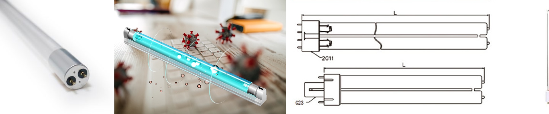
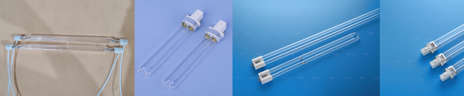
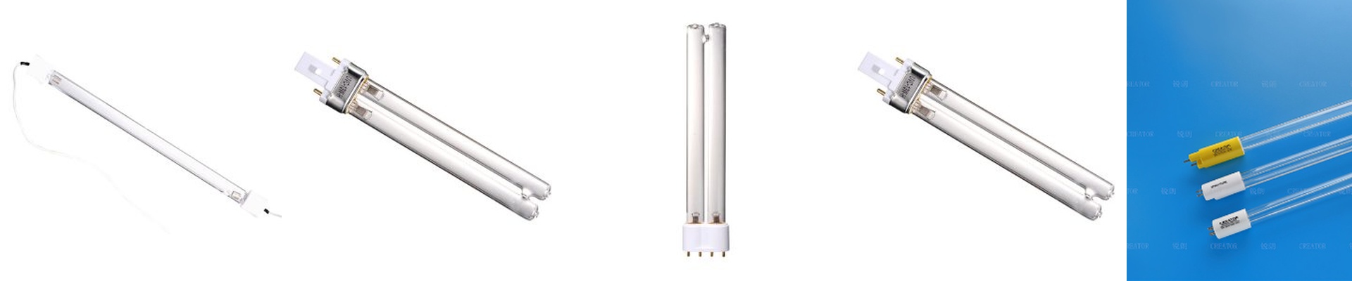
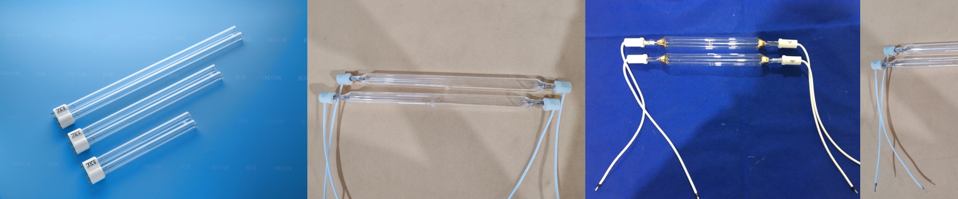
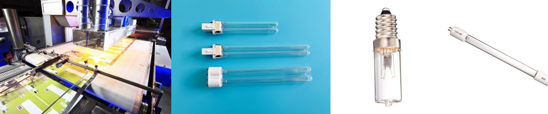
On the PCB line, that thin solder mask has to cure all the way through the micro-circuitry—no bridging, no under-cure. If the UV energy doesn’t match the photoinitiator profile, you’ll see adhesion loss, bridging, and latent electrical failures. So yes, yield is directly tied to the lamp: its spectral output and how evenly it hits the board. What matters technically For solder mask on fine lines, the dominant wavelength is 365nm, right where the photoinitiator absorbs hardest. That gives you a fast surface cure and full cross-linking through the film. We run a high-pressure mercury vapor lamp with stable spectral output, a dichroic-coated reflector to maximize peak irradiance, and a controlled dose window of 500–1200 mJ/cm². Across the cure width, output uniformity stays within ±5% so you don’t under-cure the edges. Lamp output is held steady over life—less than 5% drop after 2000 hours—and ozone-free operation keeps the equipment from getting grimy. Why it works in practice In PCB exposure and curing, the lamp’s 365nm output hits the photoinitiator and sets the mask quickly, even between traces, without dumping excess heat into the laminate. Stable irradiance means repeatable line definition, less bridging, and consistent adhesion. The payoff is fewer reworks, predictable cycle times, and lower scrap. And when you’re hunting leakage, consistent curing removes the pinholes and weak cross-links that can hide tiny leak paths. That way, electrical test and in-line inspection catch defects early. Here’s what to watch Match the lamp to your printer and reflector geometry. Mismatched reflectors waste energy and create hot spots. Make sure your system can deliver the required power density without cooking the substrate. Plan for thermal management and alignment tolerances—even a 1mm offset can shift dose by 8–10%. Also, expect a warm-up. Output stabilizes after a few minutes, so line speed and lamp warm-up need to be in sync.